When a p-type semiconductor is suitably joined to n-type semiconductor, then the system is PN junction diode. It is a two terminal semiconductor device. The contact surface where p-type and n-type meet is known as PN junction.
Circuit Symbol:

The arrow represents the direction of flow of conventional current. [Electric Current]
Formation of PN Junction Diode
The PN junction diode is not formed merely by joining the two pieces of p-type and n-type semiconductor. It is formed by diffusing one half side of p-type to another half side of n-type. Then, the p-side has many holes and the n-side has many free electrons.
As soon as the PN junction is formed, electrons from the n-side of the junction diffuse. When a free electron leaves the n-region its departure creates a positively charged atom (a positive ion) in that region. And when it enters the p-region, it fills a hole. This merging of a free electron and a hole is called electron-hole recombination. When recombination takes place, it disappears and therefore the associated atom becomes negatively charged (a negative ion).

Thus, when an electron diffuses across the junction, it creates a pair of ions. These ions are fixed in the crystal structure because of covalent bonding and cannot move freely like electrons and holes. As the number of ions increases, the region near the junction is depleted (emptied) of free electrons and holes. This small region on both sides of the junction is called depletion layer.
Now, when a free electron in the n-region tries to diffuse into the p-region, it gets repelled back by the negative wall of ions. Only the free electron, which has enough energy to break the wall of ions, fills a hole and creates another negative ion. The strength of the depletion layer keeps on increasing when an electron gets diffused. It happens until equilibrium is reached where the repulsion of the depletion layer stops the further diffusion of free electrons across the junction.
Finally, in the depletion layer, the stakes of positive ions on the n-side and the negative ions on the p-side at a distance forms an electric field called as Barrier Field. This collection of positive and negative charges at the junction sets up p.d. across the junction which is called potential barrier. Its value depends on the nature of the crystal, its temperature and the amount of doping. Potential barrier for silicon diode is 0.7 V and for germanium diode is 0.3 V. When temperature increases more minority charge carriers are created which causes the diffusion to stop at lower potential barrier. Outside the barrier on each side of the junction, the material is still neutral. There is positive charge on n-side and negative charge on p-side only inside the barrier.
Biasing of a PN Junction Diode
Biasing of PN junction means the process of applying pd across it. Biasing can be done in two ways; forward biasing and reverse biasing.
Forward Biasing
In this biasing, the positive terminal of the battery is connected to the P-type region and the negative terminal is connected to the N-type region.
The negative terminal of the battery repels the free electrons in the N-region towards the junction and the positive terminal also pushes the holes towards the junction. In this way, free electrons and holes combine at the junction. For each combination, a free electron leaves the battery and enters the n-region, also a valence electron leaves the p-region and goes to the battery. So, a current flows through the diode which is known as forward current.

Features of forward biasing:
- The potential barrier is reduced.
- The junction offers low resistance to the current and this resistance is known as forward resistance.
- Within the diode, the current is due to both types of majority charge carriers but in external circuit, it is because of electron only.
- Depletion layer decreases.
Reverse Biasing
In this biasing, the positive terminal of a battery is connected to the N-type region and the negative terminal is connected to the P-type region.
The positive terminal of the battery attracts the electrons from the N-region and the negative terminal attracts the holes from the P-region. The departing electrons leave more positive ions near the junction and the departing holes leave more negative ions near the ions. As a result, the depletion layer gets wider. The depletion layer grows until the p.d. across it equals the applied voltage and then free electrons and holes stop moving.

In this biasing, a small current exists in the circuit which is due to the minority charge carriers. The free electrons in the P-region and the holes in the N-region are minority charge carriers. These minority charge carriers are pushed towards the junction where they recombine which allows electrons to enter and leave the diode. As a result, current is constituted which is known as reverse current (leakage current).
Features of reverse biasing;
- The potential barrier increases.
- The depletion layer increases.
- The junction offers very high resistance and this resistance is known as reverse resistance.
- The value of reverse current is negligibly small.
Characteristics of a PN Junction Diode
Forward Characteristics
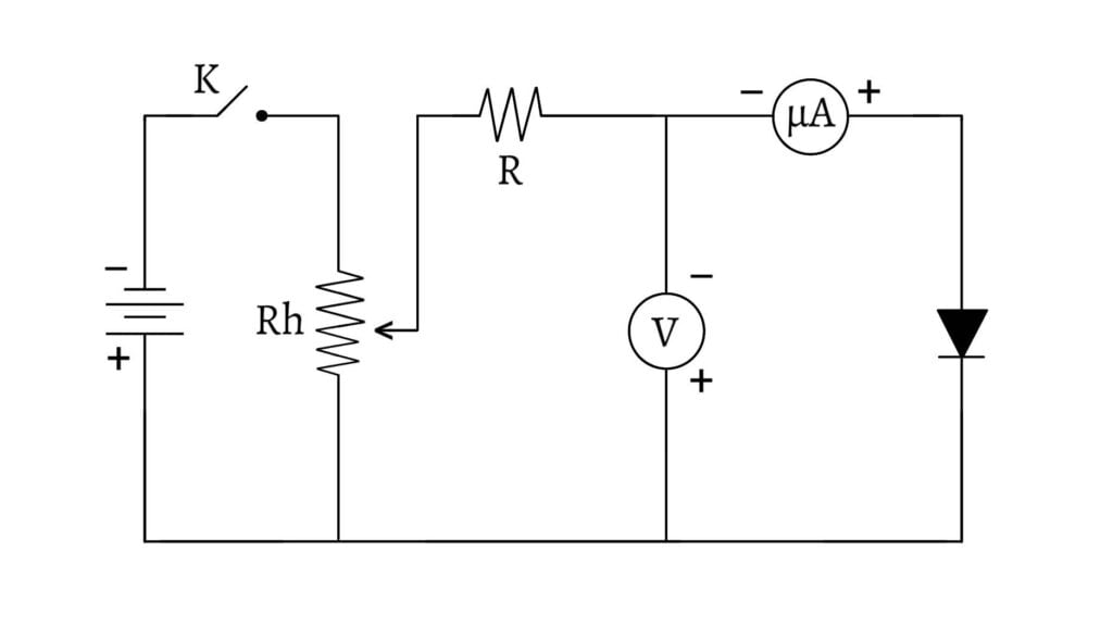
Forward characteristics of a junction diode are studied by forward biasing of the diode. It can be studied by varying resistance with the help of rheostat and varying voltage across the diode by which current also varies. For each value of the voltage across the junction, the corresponding currents are measured and then the voltage-current graph is drawn.

In forward biasing, the junction offers low resistance. As the applied voltage is increased gradually, the forward current increases very slowly. If the applied voltage is further increased, it overcomes the potential barrier and the diode behaves like an ordinary conductor. As a result, the current rises almost sharply with increase in voltage. The forward voltage at which the current starts to increases rapidly is known as knee voltage or offset voltage (Vk). Vk for Si diode is 0.7 V and for Ge diode is 0.3 V.

Reverse Characteristics
Reverse characteristics of a junction diode are studied by reverse biasing of the diode. It can be studied by varying resistance with the help of rheostat and varying voltage across the diode by which current also varies. For each value of the voltage across the junction, the corresponding currents are measured and then the voltage-current graph is drawn.
In reverse biasing, the junction offers very high resistance. As the applied voltage is increased gradually, the reverse current increases very slowly (almost constant). Then, at a particular voltage, the junction is broken down with sudden rise in current. This particular voltage is known as breakdown voltage (Vb). The breakdown voltage depends on the doping and the width of the depletion layer. Once the breakdown voltage is reached, the high reverse current may damage the junction permanently and it cannot be used again. The diode which works in the breakdown voltage also is Zener diode.